There are three sections to our laboratory: Synthesis, Characterization and Modeling.

Synthesis

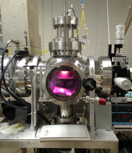
Sputtering Deposition System

Our sputtering deposition system, from NorCal, is capable of both DC and RF sputtering with 2” targets, stage rotation and two simultaneous gas mixtures.

pld
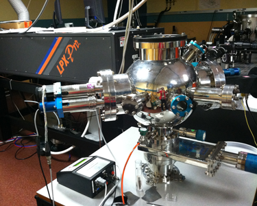
Pulsed Laser Deposition

It is used to deposit thin film on a substrate under high vacuum.
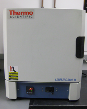
box_furnaceBox Furnaces

Materials are heated to a desired temperature in this equipment, where 1100°C is the maximum temperature.
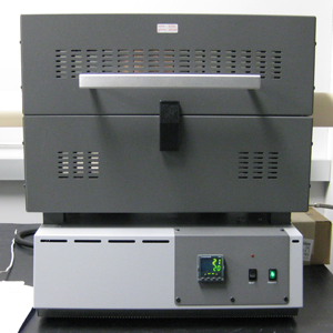
tube_furnaceTube Furnace

It is used when a constant flow of air is desired during the material heating process. It is set up with a flow meter and argon gas.
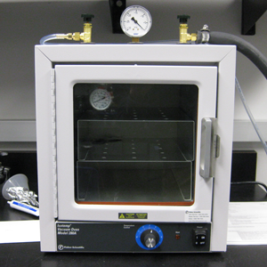
vaccuum_ovenVacuum Oven

It is used to completely dry out materials before it is put into the glovebox.
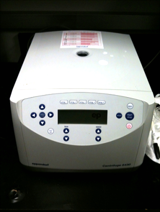
centrifugeCentrifuge

The Eppendorf centrifuge is driven by an electric motor that puts an object in rotation around a fixed axis which then separates dense substances from the media along the radial direction.
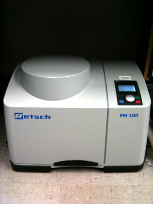
ball millPlanetary Ball Mill

This is used wherever the highest degree of fineness is required. The extremely high centrifugal forces of the planetary ball mills result in very high pulverization energy; therefore, short grinding times. The final fineness is smaller than 0.1μm.
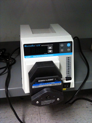
mini pumpMini-flow Pump

This is in the ultra low flow range pump, used in the coprecipitation synthesis of materials. The speed can be controlled, and the flow can be reversed if necessary.
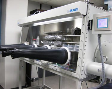
Characterization

gloveboxGlovebox

Coin cell and Swagelok cell batteries are assembled in here. Conditions are adjusted so that the electrolyte and lithium are well maintained.

arbin_instruments
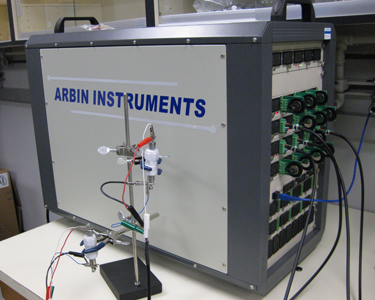
Multichannel Battery Cycler

LESC has three Arbin Instrurments  BT2000 having a total of 92 channels. Charge/Discharge, Cycling, and PITT tests are done on this equipment.

solartron
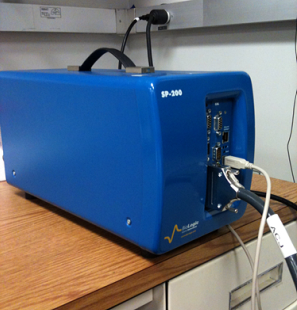
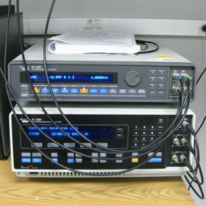
Solartron Impedance / Gain-Phase Analyzer

Electrochemical impedance spectroscopy (EIS) measurement of the battery is done on this equipment.

uv_spectrophotometer
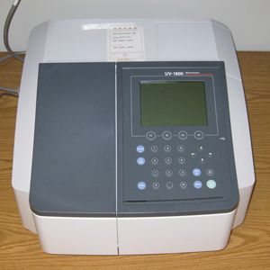
UV spectrophotometer

Absorbance and transmittance of the dye-sensitized materials at certain wavelengths are measured through this equipment.
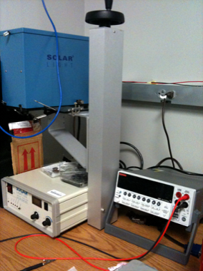
solarSolar Simulator

This instrument consists of a Xenon light source and the power supply. The efficiency of the perovskite-sensitized solar cells (PSSCs) can be measured by this equipment.

RDE_2
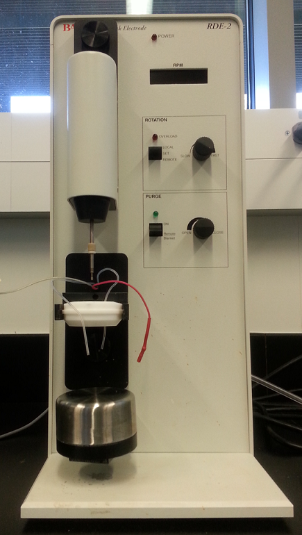
Basi Rotating Disk Electrode

The RDE is a rotator system for both fixed rotation rate and hydrodynamic modulation rotating disk electrochemical experiments. It is used to investigate reaction mechanisms related to redox chemistry.

potentiostateLow Current Potentiostat

This research grade potentiostat features a low current option capable of applying current down to 1 pA with
femto-amp accuracy.

Modeling

5
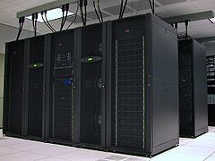
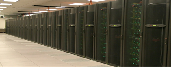
Texas Advanced Computing Center (TACC) resource-Stampede

Processors: 2/8-core Xeon E5 processors, 1/61-core Xeon Phi coprocessor
Memory: 32GB/node
Network: InfiniBand Mellanox Switches/HCAs
Hard Drive: SATA (250GB)/node

1San Diego Supercomputer Center (SDSC) resource – TACC

Processors: Dual-socket, 12-core, 2.5GHz Intel Xeon E5-2680 and Dual-socket, 8-core, 2.6GHz Intel Xeon E5-2670
Memory: 64 – 256GB/node
Network: 10GbE (QDR InfiniBand optional)
Hard Drive: 500GB onboard (second hard drive or SSD optional)/node

1Argonne National Laboratory (ANL) resource – Carbon

Processors: Xeon E5355, E5540, E5645, and E5-2650 v2 processors
Memory: 2 – 8GB/node
Network: Infiniband DDR/QDR
Hard Drive: 160 – 250 GB/node

Shared Facilities

CMRR Materials Characterization Facility 

The facility provides access to an array of state-of-the-art equipment for nanomaterial (both thin-film and powder) characterization, including XRD, XPS, Hall effect, UV-Vis, AFM/MFM, SEM, and photo current systems to measure crystal structure, and magnetic, surface, transport, and optical properties.

Nano3 Cleanroom

The California Institute of Telecommunications and Information Technology (Calit2) operates the Nano3
(Nanoscience, Nanoengineering, Nanomedicine) Clean Room facilities. The facility operates 12,000
square feet of clean rooms area from class 100 to class 1000. This recharge facility has a fully operational
photolithography, different types of evaporators, etchers, a recently installed state of the art electron beam
writer, several new state of the art mask changers, new reactive ion etchers, fully operational scanning
probe systems, and a variety of other ancillary equipment. In order to synthesize and characterize novel electrode materials LESC utilizes:

Atomic force microscopy: Atomic resolution images of material of interest are obtained through the use of this equipment.

Optical microscope:  Here high resolution digital imaging can be obtained that range from 5x to 150x.

Plasma Dry Etching:   The Oxford Plasmalab 100 RIE/ICP uses fluorinated chemistry such as Ar, O2, CHF3, CF4,C4F8,  and SF6 to remove unwanted layers of materials.

Ellipsometer: This instrument is critical in obtaining the silicon oxide layer thickness that forms on a silicon wafer.

Metalization / Thin Film Deposition: This is used to sputter thin films of conductive metals onto various electrodes.

Scanning Electron Microscope: It is used to obtain information on the materials’ surface topography, composition, and others such as electric conductivity.

 The Laboratory for Electron and X-ray Instrumentation (LEXI)

This is a university-wide shared user facility located at University California Irvine, focusing on the investigation of crystal structure, surface topography, materials microstructure and chemical microanalysis. Here LESC takes advantage of the Focused Ion Beam (FIB).

 Scripps Institution of Oceanography UC San Diego

This is a shared facility where LESC conducts Inductively Coupled Plasma-Optical Emission Spectroscopy (ICP-OES).

The NanoEngineering Materials Research Center (NE-MRC)

Located in the basement of the Structure and Materials Engineering building at UCSD, this center contains an array of equipment and instruments covering a broad spectrum of materials characterization, synthesis, and testing capabilities which include:

XRD system: It is use to analyze the phases of the material, composition, and some macroscopic information like
crystallite size. Initial assessment of the material is usually done on this equipment.

Scanning transmission electron microscope: High resolution mapping at atomic level is possible with the incorporationof analysis techniques such as EELS, ADF, and EDX.

Differential Scanning Calorimetry (DSC):  This is a thermoanalytical technique in which the difference in the
amount of heat required to increase the temperature of a sample and reference is measured as a function of temperature. It features the fastest controlled heating and cooling rates, fastest equilibration for isothermal analysis, and calibration constancy.

Thermogravimetric/Differential Thermal Analysis (TG-DTA): This provides simultaneous measurements of the thermogravimetric (TGA) and differential thermal analysis (DTA) of materials.The instrument uses a dual balance beam design, which provides very stable TGA measurements and allows for the determination of
the DTA response of the sample. The DTA signal is obtained with the incorporation of a thermocouple directly under the sample and reference measurement platforms.

Fourier Transform Infrared Spectroscopy (FT-IR) : This is a technique which is used to obtain an infrared spectrum of absorption, emission, photoconductivity or Raman scattering of a solid, liquid or gas. It is capable of data collection over a wavenumber ranged of 350 – 8300 cm-1.

 Ultraviolet-Visible-Near Infrared Spectroscopy (UV-VIS-NIR):  This provides ultra-high UV/Vis/NIR performance for wavelengths up to 3300 nm with extreme sensitivity in the NIR region (800-2500 nm) and higher energy throughput. For applications such as highly reflective and anti-reflective coatings, all types of glass from clear to highly absorbing safety glass, optical filters of all types from the deep UV through the NIR and many more applications requiring the best photo-dynamic range and the widest possible sampling capability.

Raman Spectroscopy (RAMAN): This is a spectroscopic technique used to observe vibrational,
rotational, and other low-frequency modes in a system. Excitation source is 350 mW near infrared 785 nm laser; delivering100 mW at the sample. This instrument has a spectral range  of 95 – 3500 cm-1 Raman shift.

Scanning Transmission Electron Microscopy (STEM) with Energy-Dispersive X-ray spectroscopy (EDX):
STEM is distinguished from conventional transmission electron microscopes (CTEM) by focusing the electron beam into a narrow spot which is scanned over the sample in a raster.