Synthesis

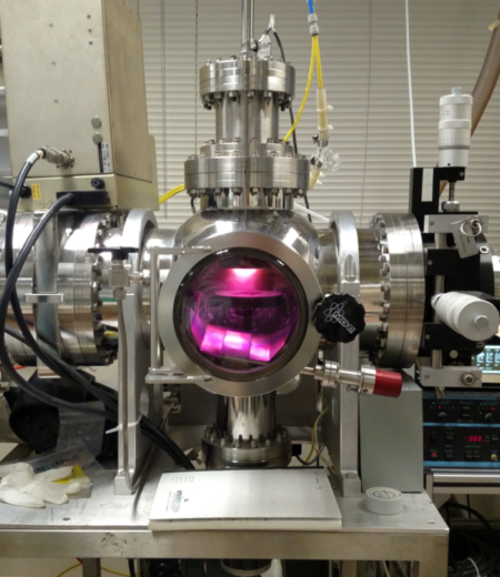
Sputtering Deposition System

Our sputtering deposition system, from NorCal, is capable of both DC and RF sputtering with 2” targets, stage rotation and two simultaneous gas mixtures.

pld
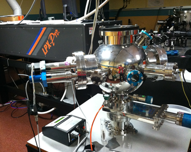
Pulsed Laser Deposition

It is used to deposit thin film on a substrate under high vacuum.
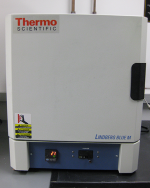
box_furnaceBox Furnaces

Materials are heated to a desired temperature in this equipment, where 1100°C is the maximum temperature.
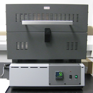
tube_furnaceTube Furnace

It is used when a constant flow of air is desired during the material heating process. It is set up with a flow meter and argon gas.
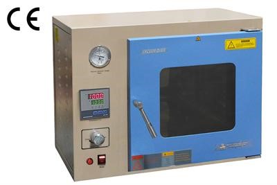
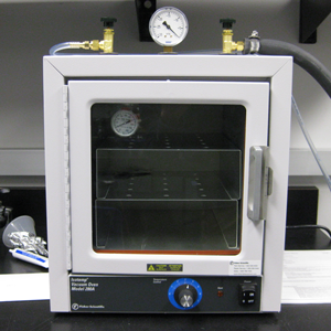
vaccuum_ovenVacuum Oven

It is used to completely dry out materials before it is put into the glovebox.
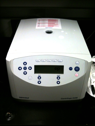
centrifugeCentrifuge

The Eppendorf centrifuge is driven by an electric motor that puts an object in rotation around a fixed axis which then separates dense substances from the media along the radial direction.
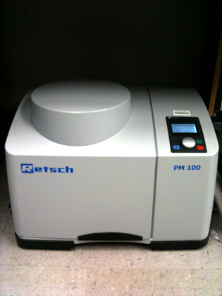
ball millPlanetary Ball Mill

This is used wherever the highest degree of fineness is required. The extremely high centrifugal forces of the planetary ball mills result in very high pulverization energy; therefore, short grinding times. The final fineness is smaller than 0.1μm.
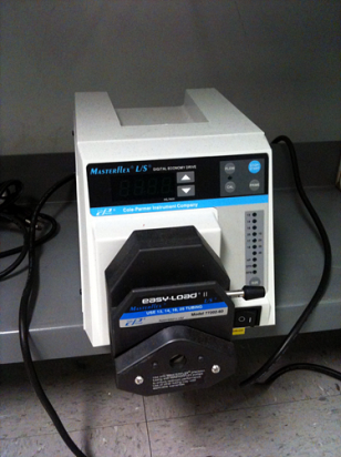
mini pumpMini-flow Pump

This is in the ultra low flow range pump, used in the coprecipitation synthesis of materials. The speed can be controlled, and the flow can be reversed if necessary.
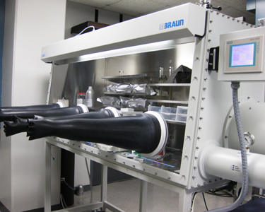
Characterization

gloveboxGlovebox

Coin cell and Swagelok cell batteries are assembled in here. Conditions are adjusted so that the electrolyte and lithium are well maintained.

arbin_instruments
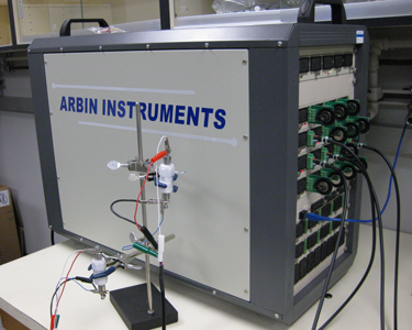
Multichannel Battery Cycler

LESC has three Arbin Instrurments  BT2000 having a total of 92 channels. Charge/Discharge, Cycling, and PITT tests are done on this equipment.

solartron
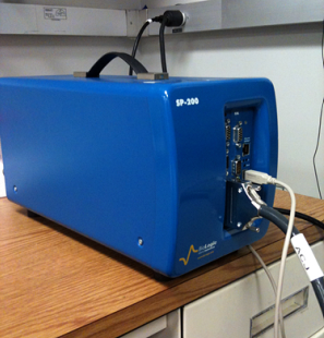
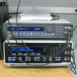
Solartron Impedance / Gain-Phase Analyzer

Electrochemical impedance spectroscopy (EIS) measurement of the battery is done on this equipment.

uv_spectrophotometer
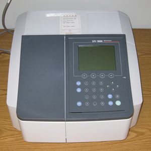
UV spectrophotometer

Absorbance and transmittance of the dye-sensitized materials at certain wavelengths are measured through this equipment.
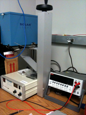
solarSolar Simulator

This instrument consists of a Xenon light source and the power supply. The efficiency of the perovskite-sensitized solar cells (PSSCs) can be measured by this equipment.

RDE_2
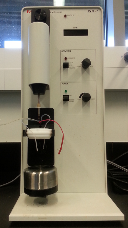
Basi Rotating Disk Electrode

The RDE is a rotator system for both fixed rotation rate and hydrodynamic modulation rotating disk electrochemical experiments. It is used to investigate reaction mechanisms related to redox chemistry.

potentiostateLow Current Potentiostat

This research grade potentiostat features a low current option capable of applying current down to 1 pA with
femto-amp accuracy.

Battery Prototyping

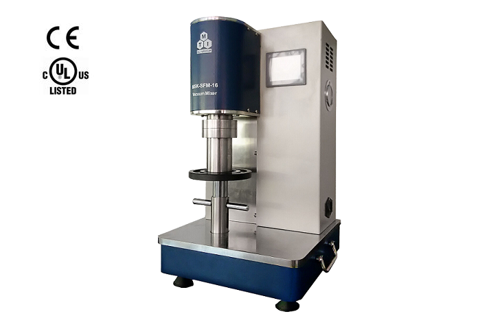
Compact Dual-Shaft Planetary Vacuum Mixer

  • A high-quality mixer tool for preparing battery electrode paste
  • Programmable mixing speed from 0-600 rpm, mixing time from 0-600 minutes
  • Built-in pump for gas removing, -0.08 ~ -0.09 MPa
  • 50-150 mL electrode paste loading

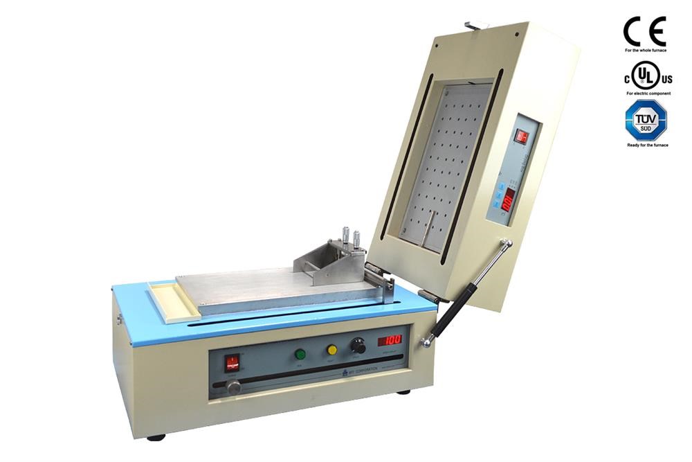
Compact Tape Casting Coater

  • A compact tape casting coater with vacuum chuck, adjustable film applicator and optional dryer cover
  • Traverse speed is adjustable from 10 – 100 mm/s
  • Stroke length is adjustable from 10 – 250 mm
  • Vacuum chuck dimension 365 mm (L) * 200 mm (W)
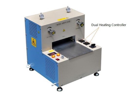
Hot Rolling Press

  • For calendaring battery electrodes to increase material density anf achieve better surface quality
  • 8″ Dia * 10″ Width (200 mm D * 250 mm W)
  • Up to 80 oC
  • The gap between two tool rollers is adjustable from 0 ~ 2 mm

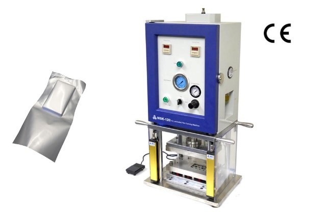
Pouch Cell Case/Cup Forming Machine

  • It is used to prepare polymer cases made of Al laminated films
  • 85 mm (L) * 60 mm (W)
  • Adjustable H 3/4/5/6 mm


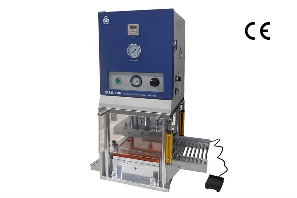
Semi-Automatic Die Cutter

  • A necessary tool in the production line of pouch cell to produce specific shapes of cathodes and anodes with current collector tabs
  • Cathode Die: 56mm (L) * 43mm (W). With 10mm (L) * 10mm (W) protrude current collector
  • Anode Die: 58mm (L) * 45mm (W). With 10mm (L) * 10mm (W) protrude current collector

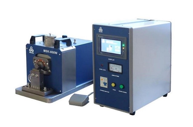
Desk-Top 800W Ultrasonic Metal Welder (Tabbing) with Touch-Screen Digital Controller

  • It is designed for welding stacked electrode sheets (Cu and Al) and tabs onto current collectors to prepare pouch cells
  • Adjustable welding time, delay time and welding layers
  • Preset welding programs selectable for Cu and Al
  • 15 layers Max.
  • Welding area 4 mm * 4 mm

UL Standard Vacuum Oven with Programmable Controller

  • Inner chamber size 16.3” * 13.5” * 14.5”
  • Capacity 53 L
  • RT – 200 oC for continuous; 200 – 250 oC for less than 4 hours

Semi-Auto Stacking Machine for Pouch Cell Electrodes

  • With “Z” fashion stacking method, anode and cathode electrodes are alternatively stacked with separator in between
  • Stacking electrode size 230 mm * 150 mm Max.; 44 mm * 44 mm Min

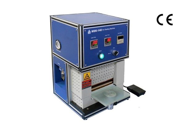
Compact Heating Sealer

  • For sealing laminated Al case during pouch cell preparation
  • Sealing width 3.2 mm
  • Sealing length 190 mm Max.
  • Sealing thickness 0 – 0.5 mm

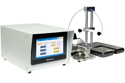
Desk-top Precision Electrolyte Filler

  • The filter with speed control console and injection pump is for high-precision electrolyte injection
  • Filling volume range 0 – 2.5 mL
  • Increment 5 µL/Thou
  • Digital scale accuracy 0.01g

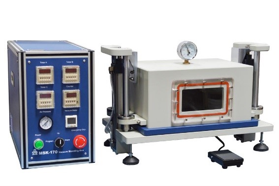
Electrolyte Diffusion & Degassing Chamber

  • For removing gas from the electrolyte after it is injected into the pouch cell and after the formation for final sealing under vacuum contain
  • Unique periods of vacuum control system allow electrolyte to thoroughly saturate the electrodes

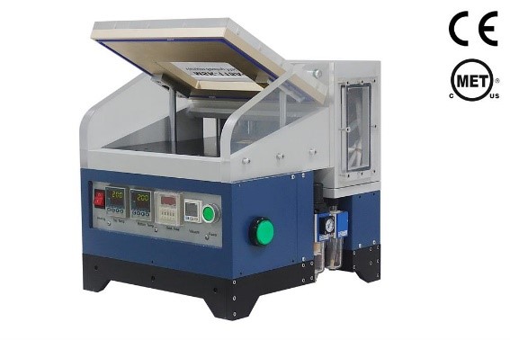
Compact Vacuum Sealer with Integrated Temperature and Pressure Control

  • A vacuum sealer for sealing Al-laminated case for pouch cell in a glove box
  • Integrating temperature, pressure and duration control
  • Vacuum range -95 ~ 0 kPa
  • Max battery size 160 mm in length and width, 12 mm in thickness

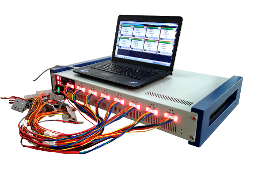
8 Channel Battery Analyzer

  • 10 mA – 5000 mA
  • Up to 5 V
  • Accuracy ± (0.05% RD + 0.05% FS)
  • Resolution 0.1 mA

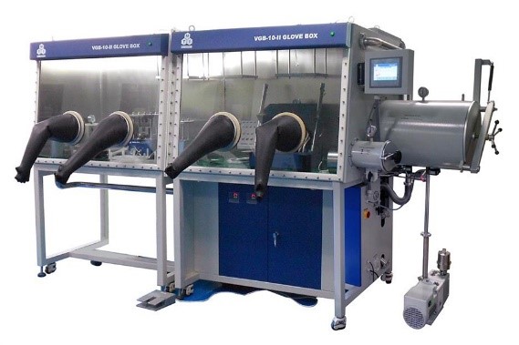
Dual Chamber Glove Box (94″ x 31″ x 36″) with Gas Purification System

  • Purification cylinder is made of BASF antioxidant materials and UOP water adsorbent materials to achieve low water and oxygen concentration
  • H2O & O2 < 1ppm

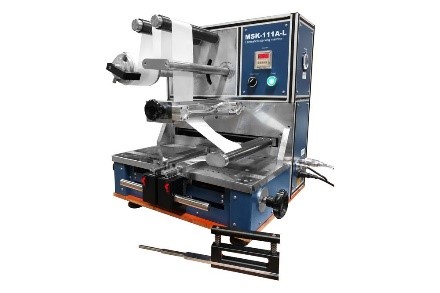
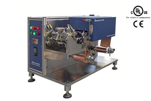
Compact Roll to Roll Blade Coating System with Drying Oven

  • A continuous coater for battery electrode sheets
  • Integrating functions of reeling in & out, slurry feeder, coating blade, baking oven and final electrode winding
  • Maximum 160 mm in width and 500 m in length automatically

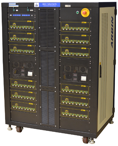
Arbin Ultra-High Precision Laboratory Battery Testing System

  • Model: LBT21084, LBT-5V-5A
  • 96 channels
  • Voltage range 0 – 5 V
  • Current ranges ±5A/500mA/20mA/1mA
  • Voltage/Current measurement resolution <10µV/0.0003% (as low as 6nA)
  • Voltage/Current measurement precision < 100ppm/<100ppm
  • Minimum step time 5 ms
Lithium Metal Workstation

Modeling

5Texas Advanced Computing Center (TACC) resource-Stampede

  • Processors: 2/8-core Xeon E5 processors, 1/61-core Xeon Phi coprocessor
  • Memory: 32GB/node Network: InfiniBand Mellanox Switches/HCAs
  • Hard Drive: SATA (250GB)/node

1San Diego Supercomputer Center (SDSC) resource – TACC

Processors: Dual-socket, 12-core, 2.5GHz Intel Xeon E5-2680 and Dual-socket, 8-core, 2.6GHz Intel Xeon E5-2670
Memory: 64 – 256GB/node
Network: 10GbE (QDR InfiniBand optional)
Hard Drive: 500GB onboard (second hard drive or SSD optional)/node

1Argonne National Laboratory (ANL) resource – Carbon

Processors: Xeon E5355, E5540, E5645, and E5-2650 v2 processors
Memory: 2 – 8GB/node
Network: Infiniband DDR/QDR
Hard Drive: 160 – 250 GB/node

Shared Facilities

The facility provides access to an array of state-of-the-art equipment for nanomaterial (both thin-film and powder) characterization, including XRD, XPS, Hall effect, UV-Vis, AFM/MFM, SEM, and photo current systems to measure crystal structure, and magnetic, surface, transport, and optical properties.

  • Hitachi UH4150 UV-Visible/NIR Spectrophotometer 
  • JEOL JSM-7400F Field Emission Scanning Electron Microscope 
  • Kobelco Photocurrent Measurement System 
  • Lake Shore 8400 Series Hall Effect Measurement System 
  • Panalytical XPert XRD – Line Source
  • Panalytical XPert XRD – Point Source 
  • PHI Quantera Scanning XPS 
  • Bruker D2 Phaser Benchtop XRD 
  • Rigaku Smartlab XRD 
  • Veeco Dimension 3100 AFM/MFM 

The California Institute of Telecommunications and Information Technology (Calit2) operates the Nano3 (Nanoscience, Nanoengineering, Nanomedicine) Clean Room facilities. The facility operates 12,000 square feet of clean rooms area from class 100 to class 1000. This recharge facility has a fully operational photolithography, different types of evaporators, etchers, a recently installed state of the art electron beam writer, several new state of the art mask changers, new reactive ion etchers, fully operational scanning probe systems, and a variety of other ancillary equipment. In order to synthesize and characterize novel electrode materials LESC utilizes:

  • Atomic force microscopy from MultiMode, model MMAFMLN. Atomic resolution images of material of interest are obtained through the use of this equipment.

  • Optical microscope from Carl Zeiss, Axio Imager. It ranges from 5x to 150x, and high resolution digital imaging can be obtained.
  • Plasma Dry Etching from Oxford Plasmalab 100 RIE/ICP uses fluorinated chemistry such as Ar, O2, CHF3, CF4,C4F8,  and SF6 to remove unwanted layers of materials.
  • Ellipsometer: This instrument is critical in obtaining the silicon oxide layer thickness that forms on a silicon wafer.
  • Metalization / Thin Film Deposition: This is used to sputter thin films of conductive metals onto various electrodes.

  • Scanning electron microscopes from FEI include the Apreo and Quanta 250 ESEM. It is used to obtain information on the materials’ surface topography, composition, and others such as electric conductivity.
  • Focused Ion Beam from FEI, model Scios DualBeam. It is used to nanofabricate samples with gallium ion milling. It is capable of producing TEM samples and enabling cross sectional imaging. We have also explored the technical capabilities of electrically biasing samples within the FIB and TEM. It has cryogenic FIB capability

Irvine Materials Research Institute (IMRI) is a newly established interdisciplinary organization under the Office of Research of the University of California, Irvine (UCI). It serves as the cross-campus nexus for materials research at UCI. IMRI operates a wide range of state-of-the-art, open-access user facilities for the characterization of materials, biological samples, and devices from sub-Å to macroscopic length scales – available to all university, industry, and non-profit researchers. It offers advanced techniques and services supported with professional staff.

  • JEOL JEM-ARM300CF S/STEM, equipped with double correctors and cold field emission gun, dual large angle EDS detectors, and Gatan GIF Quantum (electron energy loss spectroscopy and energy filtered TEM), and K2 direct detection camera, and OneView camera,  exceeds atomic resolution boundaries for any commercially available S/TEMs.  Designed to meet the most advanced materials development requirements for atom-by-atom characterization and chemical mapping, the Grand ARM offers the highest level of performance.
  • JEOL-2800 is a high throughput nano-analysis field emission TEM with automated functions.  This versatile microscope features various imaging mode such as TEM (including nanobeam and CBED mode), STEM (ADF, BF), and SEM. It is also equipped with dual large angle SDD EDS, making rapid EDS mapping possible.
  • JEM-2100F is an advanced high resolution field emission electron microscope equipped with cryo-pole-piece, cold stage, and Gatan K2 direct detection camera, and OneView camera, making it ideal to study both biological and materials samples at liquid nitrogen/room temperature.
  • FEI Quanta 3D FEG is a state-of-the-art dual-beam (SEM/FIB) instrument. It is capable of high resolution surface imaging (1nm resolution at 30kV), fast composition analysis, crystal structure determination, orientation mapping, micromachining, Pt deposition, and TEM specimen preparation. It may be operated under different vacuum modes, for example, high vacuum, low vacuum and environmental (ESEM). Either dry inorganic samples or hydrated biological samples can be observed in this instrument.
  • Rigaku SmartLab is the state of the art in highly automated, fully modular, multipurpose X-ray diffractometers. This fully-loaded system features a 2.2 kW Cu tube and a high-resolution closed loop theta-theta vertical goniometer with a horizontal sample stage and a 6-position automatic sample changer. Rigaku’s patented cross beam optics (CBO) allows rapid switching between parafocusing geometry for powder samples and parallel beam geometry for thin films and epilayers. The system incorporates SAXS optics for measuring structures with d-spacings up to 100 nm in either transmission (spinning capillary) or reflection (GISAXS) mode.
  • AXIS Supra by Kratos Analytical is a high performance multi-technique surface science instrument combining high-sensitivity X-ray photoelectron spectroscopy (XPS) with Al/Ag monochromatic X-ray source, high resolution Auger electron spectroscopy (AES), ultraviolet photoelectron spectroscopy (UPS), and ion scattering spectroscopy (ISS). The Supra is capable of fast imaging XPS and AES with a spatial resolution as high as 1.0 and 0.1 micron, respectively. In addition, an integrated glove box enables air-free sample fabrication, preparation, and transfer to the Supra’s UHV preparation chamber.
  • Nano CT from Xradia VersaXRM™ 410 is the latest generation of three-dimensional (3-D) X-ray microscopy (XRM) solutions optimized for non-destructive micro tomography for heterogeneous materials. The system’s source technology and high resolution detector provide unmatched sub-micron resolution (800nm), even for large samples.

Located in the basement of the Structure and Materials Engineering building at UCSD, this center contains an array of equipment and instruments covering a broad spectrum of materials characterization, synthesis, and testing capabilities which include:

  • Differential Scanning Calorimetry (DSC):  This is a thermoanalytical technique in which the difference in the amount of heat required to increase the temperature of a sample and reference is measured as a function of temperature. It features the fastest controlled heating and cooling rates, fastest equilibration for isothermal analysis, and calibration constancy.
  • Thermogravimetric/Differential Thermal Analysis (TG-DTA): This provides simultaneous measurements of the thermogravimetric (TGA) and differential thermal analysis (DTA) of materials.The instrument uses a dual balance beam design, which provides very stable TGA measurements and allows for the determination of the DTA response of the sample. The DTA signal is obtained with the incorporation of a thermocouple directly under the sample and reference measurement platforms.
  • Fourier Transform Infrared Spectroscopy (FT-IR) : This is a technique which is used to obtain an infrared spectrum of absorption, emission, photoconductivity or Raman scattering of a solid, liquid or gas. It is capable of data collection over a wavenumber ranged of 350 – 8300 cm-1.
  • Ultraviolet-Visible-Near Infrared Spectroscopy (UV-VIS-NIR):  This provides ultra-high UV/Vis/NIR performance for wavelengths up to 3300 nm with extreme sensitivity in the NIR region (800-2500 nm) and higher energy throughput. For applications such as highly reflective and anti-reflective coatings, all types of glass from clear to highly absorbing safety glass, optical filters of all types from the deep UV through the NIR and many more applications requiring the best photo-dynamic range and the widest possible sampling capability.
  • Raman Spectroscopy (RAMAN): This is a spectroscopic technique used to observe vibrational, rotational, and other low-frequency modes in a system. Excitation source is 350 mW near infrared 785 nm laser; delivering100 mW at the sample. This instrument has a spectral range  of 95 – 3500 cm-1 Raman shift.
  • XRD system: It is use to analyze the phases of the material, composition, and some macroscopic information like crystallite size. Initial assessment of the material is usually done on this equipment.
  • Scanning Transmission Electron Microscopy (STEM) with Energy-Dispersive X-ray spectroscopy (EDX): STEM is distinguished from conventional transmission electron microscopes (CTEM) by focusing the electron beam into a narrow spot which is scanned over the sample in a raster.
  • ICP – Optical Emission Spectrometer from Perkin Elmer, model 3700 Optical Emission Plasma Spectrometer with AS90 Autosampler, is capable of axial or radial emission measurements. This instrument is used for a wide range of minor, major and trace elements determinations, and has a resolution of 0.001 nm, spectral range between 200 – 782 nm, and can measure sample concentrations from 1-1000ppb
  • Spark Plasma Sintering (SPS) from Thermal Technology LLC is used to process powder material into a dense sample. In contrast to conventional hot-pressing which heat samples by contact or radiative heating, the SPS can rapidly heat the sample via Joules heating, reaching temperatures of 2000C in minutes. Relative sample densities upwards of 95% can be achieved in a fraction of the time compared to convention pressure-heating techniques.

  •  Inductively Coupled Plasma-Optical Emission Spectroscopy (ICP-OES). The facility houses two Thermo Fisher Scientific™ iCAP™ Qc ICP-MS instruments. One is dedicated to performing the analysis of samples in solution, the other to performing direct analysis of solid samples by laser ablation. Application types include but are not limited to biological, environmental and geological analyses. ICP-MS instruments can rapidly measure almost the entire Periodic Table simultaneously at a wide range of concentrations (sub ppb to ppm). The facility has the capability to prepare certain sample solutions if required. Both solution and laser instruments are available on a recharge basis.